Do you have any questions?
|
Technical sales iselRobotik Andreas Möller
|
 |
|
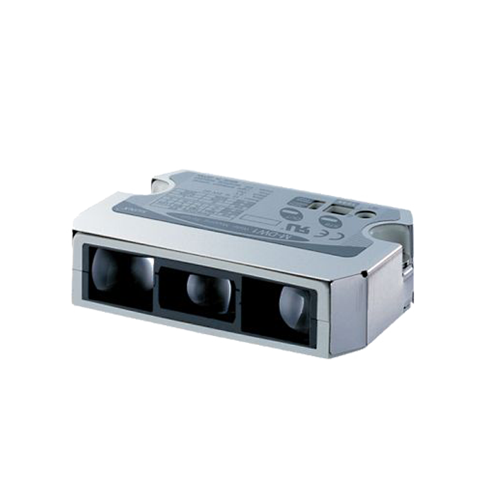
Wafer Mapping Sensor IMS-MDW1
- LED light source
- Measuring distance 45 mm (1,75")
- PNP / NPN switchable
The wafer mapping sensor which has been specifically designed for the semiconductor industry works using a double triangulation principle and has a measuring distance of 45 mm. The focussing transmitter optics and the innovative dual-segment receiver element ensure that the position of wafers (> 3 inches) is detected precisely regardless of their thickness and coating.
The areas of application for this triangulation sensor include processing technology (e.g. wafer painting and exposure machines etc.) in the semiconductor and micro-electronics industry.


